Overview
This project implements a complete Whack-A-Mole style game with the core gameplay running in hardware on an FPGA. The system cycles “moles” on LEDs, accepts player hits from physical buttons, and updates score and timing outputs deterministically. A PC-side demo pipeline (UART + GUI) was used to showcase gameplay state and validate correctness during development.
What I built
A modular Verilog design: clock division, debouncing, mole generation, game FSM, scoring/7-seg output, and a demo-friendly interface for testing.
Why it matters
FPGA projects reward discipline: timing, clean state design, and robust input handling. This was a full-stack hardware demo from signals to user experience.
Architecture
The design is organized as small, testable blocks that feed a central game FSM. A clock divider creates stable update rates (game tick / mole tick). Debouncers turn noisy button presses into single clean pulses. The FSM decides when the game is active, when a mole is “up,” and how scoring updates. Output logic drives LEDs and the 7-segment display consistently.
Signal flow
Buttons → Debounce/Pulse → FSM → Score + Mole State → LEDs / 7-seg
Design goals
Deterministic timing, no double-counted hits, and a clean separation of timing/state/display.
Hardware
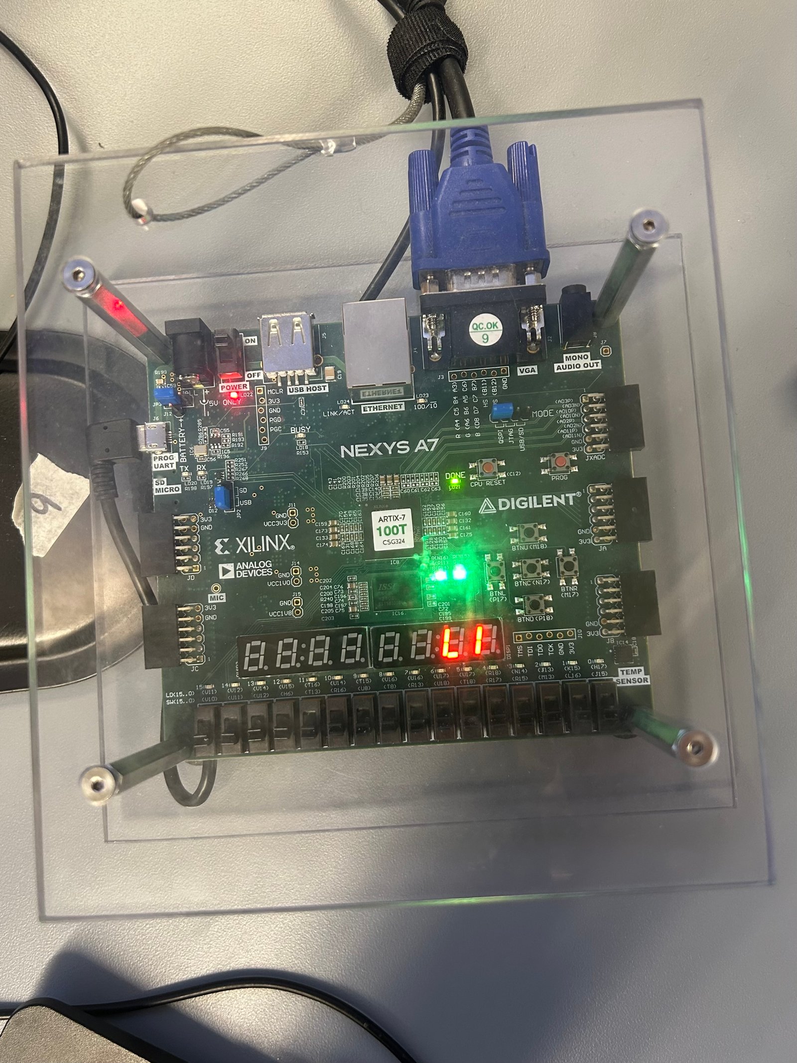
Built and demoed on a Digilent Nexys A7 FPGA platform. The physical interface uses onboard buttons as mole-hit inputs, LEDs as mole indicators, and a 7-segment display for score/time feedback.


Software
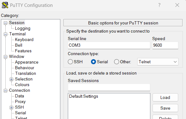
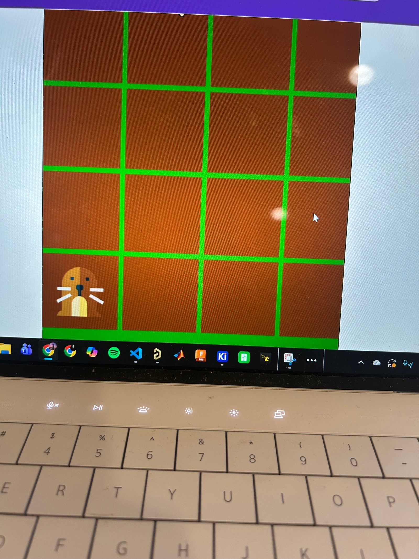
A PC-side pipeline supported rapid debugging and demo polish. UART interface using the pre-built FPGA's FTDI chip, acting as an available virtual COM port to communicate to the PC via Micro USB B bypass, allowed for state/score visibility and physical mouse to monitor interaction, using custom GUI, which helped validate timing behavior and game logic while iterating on the FPGA design.

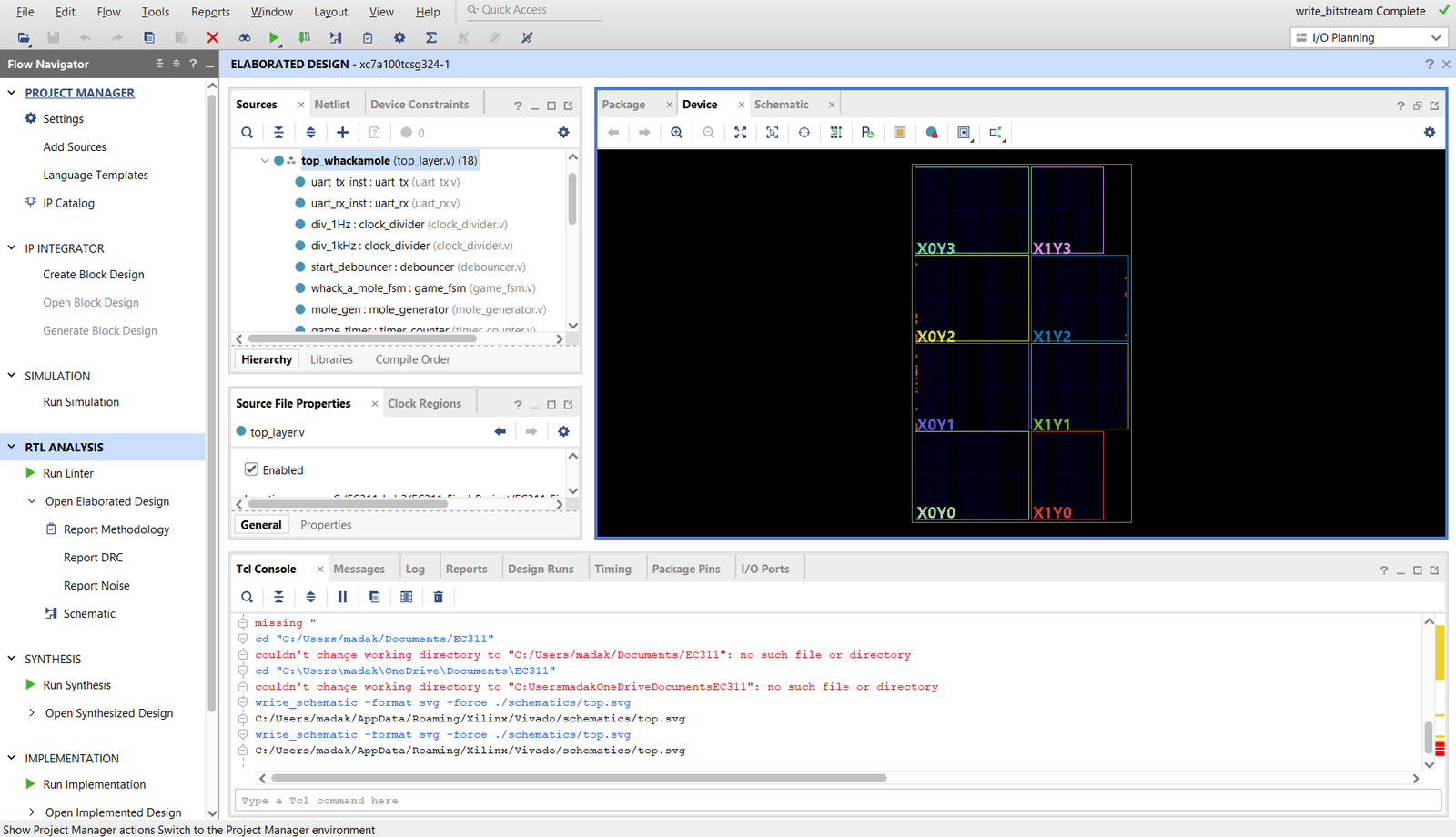
Schematic
Interactive Vivado schematic export. Zoom/pan with mouse wheel + drag.
Demo
Results
The final build delivers stable gameplay with reliable input detection and deterministic timing. The modular architecture made it easier to debug and iterate, especially when integrating display logic and demo instrumentation. The project was designed to feel “real” in a live demo setting: clean physical presentation, clear scoring feedback, and predictable behavior.
What worked best
Debouncing + pulse shaping eliminated double-hits and random state glitches.
Biggest engineering win
Keeping timing/state/output separated prevented “fix one bug, create two bugs” moments.
Reflection
Challenges
• Synchronizing real button inputs with game timing windows
• Debugging state transitions without overcomplicating the FSM
• Making the demo consistent across real-world button behavior
What I learned
• Hardware UX matters: debouncing is not optional
• Modular Verilog scales better than monolithic designs
• Instrumentation (debug LEDs / UART hooks) saves hours
 by Justin Yu